(Download) UPSC IES Exam Paper - 2018 "Electronics and Tele Communication Engineering Paper - 1"
![]()
(Download) UPSC IES Exam Paper - 2018 "Electronics and Tele Communication Engineering Paper - I"
Exam Name: Engineering Services Exam (IES)
Paper : Electronics and Tele Communication Engineering Paper - I
Year: 2018
File Type: PDF
Electronics and Tele Communication Engineering
Paper - I
Time Allowed : Three Hours
Maximum Marks : 300
QUESTION PAPER SPECIFIC INSTRUCTIONS
Please read each of the following instructions carefully before attempting questions.
Answers must be written in ENGLISH ONLY.
There are EIGHT questions divided in TWO Sections.
Candidate has to attempt FIVE questions in all.
Question Nos. 1 and 5 are compulsory and out of the remaining, THREE are to be attempted choosing at least ONE question from each Section.
The number of marks carried by a question / part is indicated against it.
Wherever any assumptions are made for answering a question, they must be clearly indicated.
Diagrams/figures, wherever required, shall be drawn in the space provided for answering the question itself.
Unless otherwise mentioned, symbols and notations carry their usual standard meanings.
Candidates should attempt all questions in the space prescribed under each question in the Question-cum-Answer (QCA) Booklet. Any answer written outside the space allotted may not be given credit.
Attempts of questions shall be counted in sequential order. Unless struck off, attempt of a question shall be counted even if attempted partly. Any page or portion of the page left blank in the Question-cum-Answer Booklet must be clearly struck off.
Values of constants which may be required:
Electron charge = -1.6 x 10⁻¹⁹ Coulomb
Free space permeability = 4p x 10-7 Henry/m
Free space permittivity = (1/36p) × 10-9 Farad/m
Velocity of light in free space = 3 x 10⁸ m/sec
Boltzmann constant = 1.38 x 10⁻²³
JK Planck's constant = 6.626 × 10⁻³⁴ J-s
SECTION ‘A’
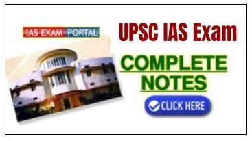
Q1. (A) Plot the output voltage of the circuit, as shown in Figure (a) below, which has as its input a sawtooth waveform depicted in Figure (b).
(C) (i) Compare accuracy and precision with an example of archery target shooting
(ii) How can time and frequency standards be disseminated ?
(D) What are Bottom-up and Top-down methods of synthesis of nano materials ?
(E). An amplifier with an open-loop gain A = 1000 + 100 is available. It is necessary to have an amplifier whose voltage gain varies by no more than +- 0.1%.
(i) Find the reverse transmission factor, B, of the feedback network used.
(ii) Find the gain with feedback.
Q2. (A) Determine the stability factor, S”, that is related to the variation of collector current Ic with respect to b, for the circuit shown below.

Assume silicon transistor and also ß to be much larger than unity.
(B) An output power of 10 W is to be delivered from a class-B push-pull amplifier. What will be the collector dissipation power of each of the transistors used ?
Instead, if another configuration of two paralleled transistors, operating in class A mode are used, what will be the collector dissipation power of each transistor ? Derive the equations used.
(C) Hall measurements are conducted on a p-type semiconductor bar 500 um wide and 20 um thick. The Hall contacts ‘A’ and 'B' are displaced 2 um with respect to each other in the direction of current flow of 3 mA. The voltage between A and B with a magnetic field of 10-5 Wb/cm2 pointing out of the plane of the sample is 3-2 mV. When the magnetic field direction is reversed the voltage changes to - 2.8 mV. Find the value of mobility of holes.
Q3. (A) Draw a schematic diagram of a solar photovoltaic cell and explain its principle of operation.
(E) A 4-pole DC generator has 1200 armature conductors and generates 250 V on open circuit when running at a speed of 500 r.p.m. The diameter of the pole-shoe circle is 0-35 m and the ratio of pole arc to pole pitch is 0.7. The length of the shoes is 0.2 m. Find the mean flux density in the air gap. Assume lap-connected armature winding.
Q4. (A) Show that the input resistance of the transistor combination shown below is much greater than that of the individual transistors.

Why is such a combination not preferred, with three or more transistors, to further increase the input resistance ?
(B) Determine the modified h-parameters of the circuit shown below.

Reduce the expressions derived above for the case if hoe Re << 1.
(C) What is the internal power of an optical source emitting at a peak wavelength of 1310 nm ? The radiative and non-radiative recombination times are 40 ns and 100 ns, respectively. The drive current is 30 mA.
Study Material for IAS (UPSC) General Studies Pre. Cum Mains
SECTION B
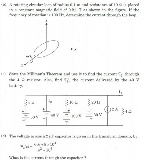
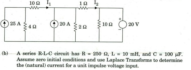
Q5. (A) Using mesh analysis and transformation of current sources to voltage sources, determine the currents I, and I, in the circuit shown below.
(C) (i) Distinguish between sensors and transducers, with examples.
(ii) What are the different constants of piezo-electric crystals ? How are they related ?
(D) NAND implementation of a circuit is to be designed with three data lines and a control line. When the control line is high, the circuit is to detect when one of the data lines has 1 on it. No more than one data line will have a 1 on it. When the control line is low, the circuit will output a 0, regardless of what is on the data line.
(E) Consider a 'Lead' material has critical temperature 7.19 K and critical magnetic flux is 0.0803 tesla. Determine the value of temperature at which 'lead' material must be cooled in a magnetic field of 15000 A/m for it to be super conductive. Assume magnetic constant value is 4p x 10-7 H/m.
Q6. (A) (i) Distinguish between thermocouples, thermistor and RTD.
(ii) Why is cold junction of thermocouples required to be compensated and how can it be compensated ?
(iii) How can you measure flow of fluid by using ultrasonic flow meter based on change in frequency (Doppler shift) ? Explain with necessary diagrams.
(B) (i) Five measurements of the resistance of a resistor gave :
101.7 W
101-0 W
101.5 W
101.2 W
and 101.1 W
Assume that only random errors are present.
Calculate :
(I) the arithmetic mean,
(II) the standard deviation of the readings,
and (III) the probable error.
(ii) Explain the signal conditioning requirements for measurements with strain gauges and how these can be achieved.
(C) The quantum efficiency of a particular silicon photo detector is 90% for the detection of radiation at a wavelength of 0-8 um. When the incident optical power is 0.8 uW, the output current from the device is 10 uA. Determine the multiplication factor of the photo detector.
Q7. (A) For the circuit shown below, calculate the currents IL, and IR:

(B) Design a counter to go through states 0, 2, 4, 5, 0 ..., using type D Flip Flops.
(C) (i) What is Spintronics ? Discuss two examples of spintronic devices.
(ii) Find the relation between unit cell edge length 'a' and atomic radius ‘r' for a body-centred cubic crystal.
(D) (i) The charge sensitivity of a piezo-electric transducer is 40 pC/N. A charge amplifier is connected with the piezo-electric transducer such that the combination of the transducer and amplifier is to have an overall gain of 100 mV/N.
Find (I) the gain of the amplifier,
(II) the value of the feedback capacitor required to have this gain.
(ii) What is telemetry ? Classify the telemetering systems.
Q8. (A) (i) What are the requirements for the processing of signals using LVDT ? Show a complete scheme to explain the displacement measurements with LVDT.
(ii) A 12 A dynamometer ammeter has a full scale deflection
of 90°. The rate of mutual inductance with deflection is constant and its value
is 0.006 uH per degree. Find the deflection, if the current to
be measured is 6 A.
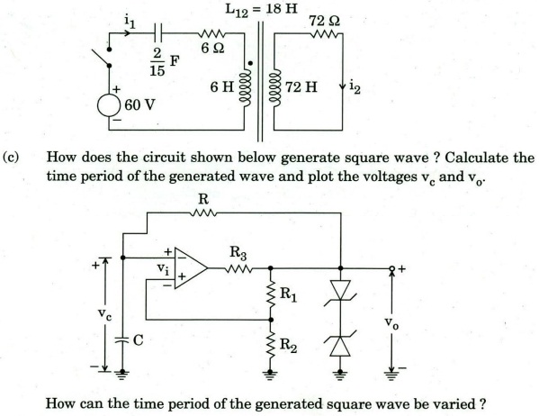
(B) An inductively coupled circuit is shown below. The switch is closed at t = 0. Assuming zero initial conditions, determine the current i2(t).